 |
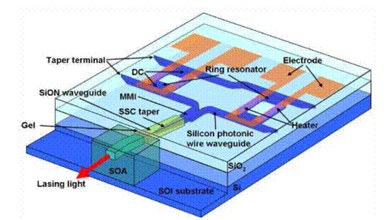
Silicon-based Laser
The laser is one of the core optoelectronic devices for silicon-based photonic integration and has been one of the research hotspots of silicon-based photonics. The integration of the silicon-based laser with the silicon-based waveguide device provides a light source. In 2009, our group's researcher Dr. Chu Tao successively developed the world's first silicon-based wavelength tunable laser and the 100nm adjustable range widest laser. In 2014, the group successfully developed silicon-based hybrid integrated lasers with self-made high-precision chip bonding equipment, with an output power of 4.2mW. This is the first time in China that a mixture of III-V series lasers and silicon-based photonic devices fabricated by standard CMOS processes has been realized. It has laid the foundation for the fabrication of silicon-based lasers using CMOS line scale. |
|
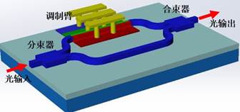 |
Silicon-based high speed electro-optic modulator
The electro-phototic modulator accomplishes the conversion function from electrical signal to optical signal and is one of the key components of optical interconnect, optical computing and optical communication systems. Silicon-based photonic devices have been the most attractive research hotspot in the field of optoelectronics in the past decade. The silicon-based electro-optic modulators have become the iconic devices representing the development level of silicon-based photonics due to their complex structure and important electro-optical conversion functions. The research team carried out systematic and in-depth research on silicon-based electro-optic modulators, and firstly realized silicon-based electro-optic modulators with modulation rates of up to 60 Gb/s, and carried out related research on packaging and other fields, ranking the world's leading level. |
|
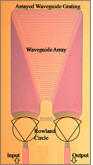 |
Silicon-based fundamental wave division multiplexing device
The wavelength division multiplexing device connects multiple lasers, modulators, detectors, etc. on the chip, so that the transmission rate and processing rate of the on-chip data can be multiplied. The EPIC group systematically studied the wavelength division multiplexing/demultiplexer, and designed and fabricated an 8×8 cyclic arrayed waveguide grating device, which achieved a minimum loss of 2.4dB and crosstalk of -17.5dB~-25.1dB. The device performance has reached the international first-class level. |
|
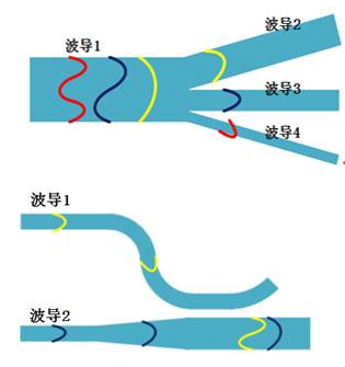 |
Silicon-based fundamental wave division multiplexing device
As a physical dimension that can carry information, on the one hand, mode can be further improved by wavelength multiplexing to further increase the number of channels. On the other hand, the number of required lasers can be reduced while maintaining the number of channels. Due to the absolute advantages of silicon-based photonic devices in terms of cost and integration, it is of great significance to carry out research on silicon-based modular multiplexer devices and systems. |
|
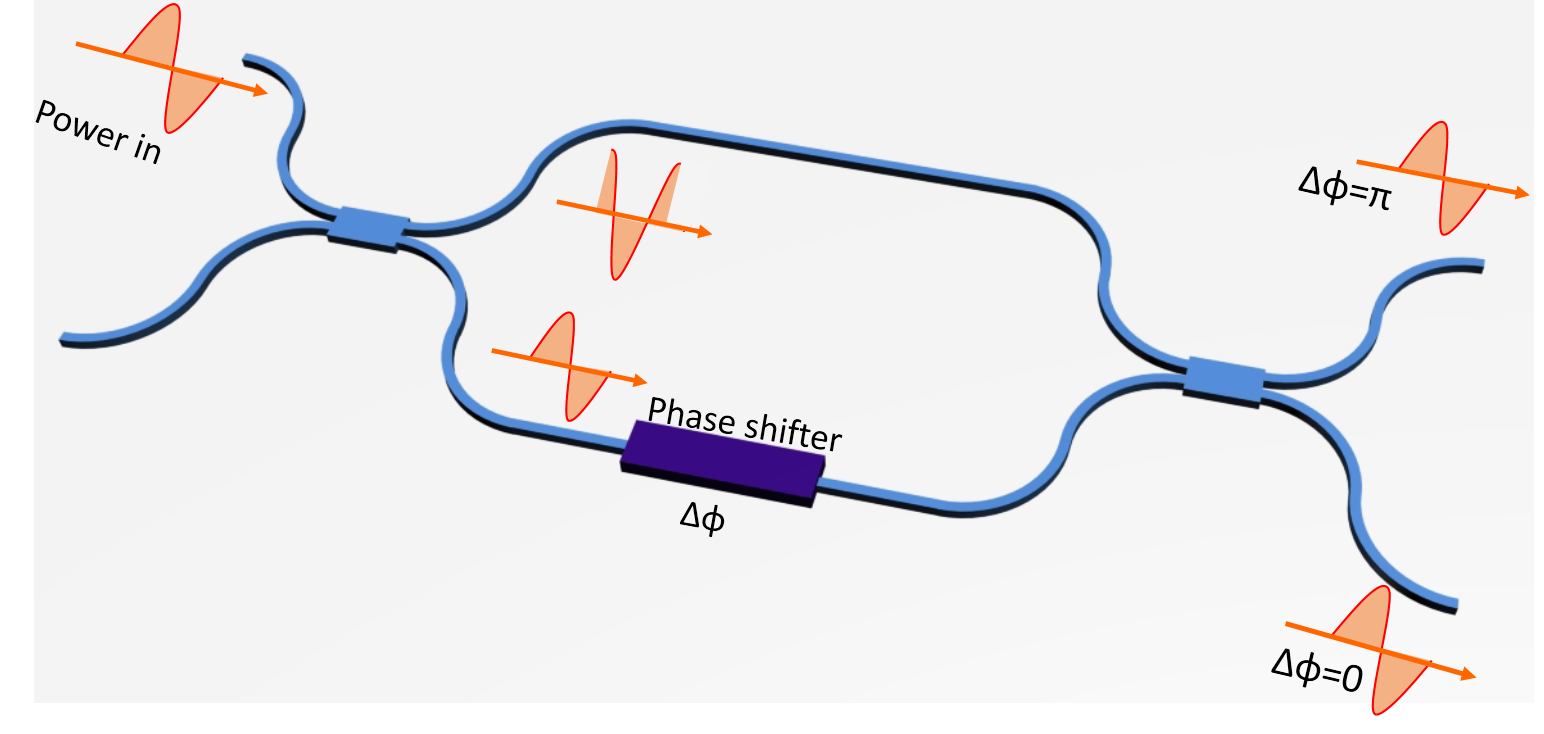 |
High-speed large-scale silicon-based optical switching array
High-speed data exchange is important in HPC and modern optical communications. In the existing optical communication network, the data exchange first converts the optical signal into an electrical signal, electrically routes the data, and re-loads the routed data on the optical transmission. Photoelectric conversion limits the transmission rate and increases the cost of data transmission. The optical switching array uses the principle of interference to control the spatial position of the light to achieve optical switching. |
|
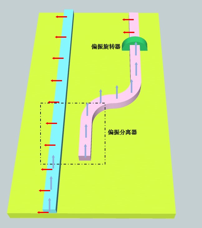 |
Polarization control device
Polarization control devices mainly include polarization splitting/combiner and polarization rotator: polarization splitting/combiner realizes separation and combination of light of different polarization states; while polarization rotator realizes the conversation between two different polarization states, such as converting the TE mode in the waveguide to a TM mode. Polarization control devices have very important applications in integrated optical paths, such as the construction of polarization diversity systems to achieve polarization-insensitive devices, and the implementation of polarization multiplexing to significantly increase the transmission rate based on existing fiber-optic cables. |
|
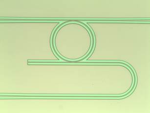 |
Silicon based filter elements
In a silicon-on-substrate optical system, the filter achieves a choice of a range of wavelengths and is a typical passive device. There are many types of components that can be used as filters, such as microring resonator structures, sidewall grating structures, Mach-Zehnder interference structures, etc. The EPIC group has the basis for designing and fabricating a variety of silicon-based filters. Taking cascaded microrings as an example, we designed and fabricated a cell device with a bandwidth of 1.8 nm and an extinction ratio of 32 dB. |
|
 |
Silicon-based integrated photodetector
Our group has extensive CMOS integration practice experience on silicon substrate detector implementation. There are currently two mature solutions: first, high-efficiency grating couplers with high-performance III-V series detectors for high-speed, high-sensitivity detection; second, integrated silicon germanium detectors on CMOS lines Although it is slightly inferior to the III-V detector in performance, it can realize large-scale, highly integrated array detection. |
|
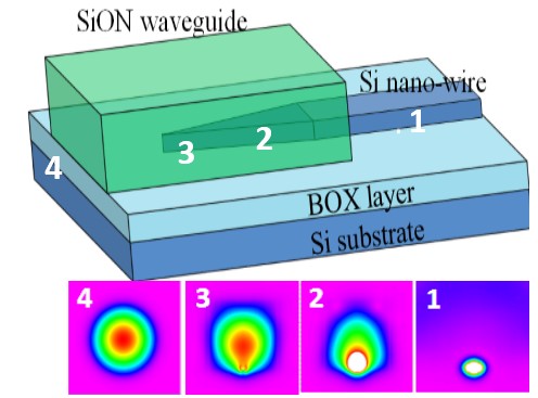 |
Silicon-based waveguide optical coupling technology
Silicon-based waveguides can converge light beams in their cores due to the high refractive index difference between the core silicon and the cladding silicon dioxide. The width of the silicon-based optical waveguide is usually around 400 nm to 500 nm, so that high-density integration of the silicon-based device can be achieved, but at the same time, the coupling between the silicon-based waveguide and the standard communication fiber is a challenge. |
|
 |
Process equipment development
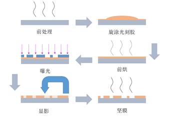
The basic method of mechanical polishing is to remove the material on the surface of the chip by mechanical grinding of abrasive grains in sandpaper or polishing liquid, and obtain a smooth surface. This technology has wide application in large-scale integrated circuit manufacturing. The lithography process plays a decisive role in the manufacture of semiconductor integrated circuits, whether it is from the capital, technology or personnel, because lithography transfers the pattern on the lithography or digital mask to the photoresist, the process, subsequent etching, deposition and other processes are based on the lithography process. |
|
|
|